Operation of FET:
Take a sample bar of N-type semiconductor. This is called as N-channel and it is electrically equivalent to the resistance as shown in the figure 1.
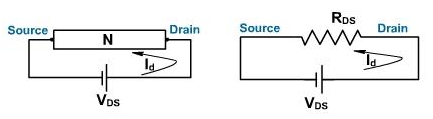
Figure 1
Ohmic contacts are added on each side of the channel to bring out the external connection. Thus if voltage is applied across the bar, current flows through the channel.
The terminal from where the majority carriers enter the channel is called as source designated by S. The terminal by which the majority carriers leave the channel is called as drain and designated by D. For the N-channel device, the majority carriers are electrons. Hence the circuit behaves like a DC voltage VDS applied across the resistance RDS. The resulting current is drain current ID. If the value of VDS increases, ID increases in proportion.
Now on both the sides of the N type bar heavily doped regions of P type impurity have been formed by any method for creating the PN junction. These impurity regions are called as gates (gate1 and gate2) as shown in the figure 2.
Both gates are internally connected to each other and they are grounded yielding zero gate source voltage (VGS =0). The word gate is used hear because the potential applied in between the gate and source controls the channel width and thus the current.

As with all the PN junctions, a depletion region is formed on two sides of the reverse biased PN junction. Current carriers have diffused across the junction, leaving only the uncovered positive ions on the n side and negative ions on the p side. The depletion region width increases with the magnitude of reverse bias. The conductivity of this channel is zero due to the unavailability of current carriers.
The potential at any point along the channel depends on the distance of that point from the drain, points closer to drain are at the higher positive potential, in relation to the ground, then points close to the source. Both the depletion regions are thus subject to greater reverse voltage near the drain. Therefore the depletion region width Fig. 2 increases as we move towards drain. Flow of the electrons from source to drain is now restricted to the narrow channel between the no conducting depletion regions. The width of this channel decides the resistance between drain and source.
Consider that the behavior of drain current ID versus the drain source voltage VDS. The gate source voltage is zero thus VGS= 0. Suppose that VDS is linearly increased linearly from 0V. The value ID also increases.
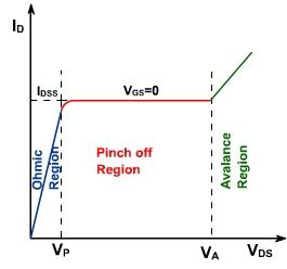
As the channel behaves as a semiconductor resistance, thus it follows ohm's law. The region is called as ohmic region, with the increasing current, ohmic voltage drop in between the source and the channel region reverse biased the junction, the conducting portion of channel starts to constrict and ID begins to level off till a specific value of VDS is reached, called as pinch of voltage VP.
At this particular point further increase in the value of VDS do not produce corresponding increase in ID. Instead, as the value of VDS increases, both the depletion regions extend further into the channel, which results in a no more cross section, and thus a higher channel resistance. Thus even if, there is more voltage, the resistance is greater and current remains relatively constant. This is called as pinch off or saturation region. The current in this region is maximum current which FET can produce and designated by IDSS.
As with all the PN junctions, when the reverse voltage exceeds a particular level, avalanche breakdown of PN junction takes place and ID rises rapidly as shown in the figure 3.
Now consider N-channel JFET with the reverse gate source voltage as shown in the figure 4.
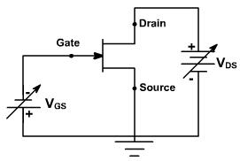
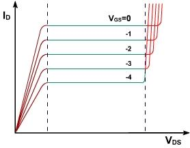
Figure 4 Figure 5
The additional reverse bias, pinch off will occur for the smaller values of | VDS |, and maximum drain current will be smaller. A family of curves for various values of VGS(negative) is shown in the figure 5.
Suppose that VGS= 0 and that because of VDS at the specific point along the channel is +5V with respect to ground. Therefore reverse voltage across either PN junction is now 5V. If VGS is decreased from 0 to -1V the net reverse bias near point is 5 - (-1) = 6V. Thus for any of the fixed value of VDS, the channel width decreases as VGS is made more negative.
Thus ID value changes correspondingly. When the gate voltage is enough negative, the depletion layers touches each other and conducting channel pinches off. In this particular case the drain current is cut off. The gate voltage which produces the cut off is symbolized VGS(off) . It is same as the pinch off voltage.
Since the gate source junction is a reverse biased silicon diode, only a very small reverse current flows through it. In the ideal conditions the gate current is zero. As a result, all the free electrons from source goes to the drain which means that ID = IS. Because the gate draws almost negligible reverse current the input resistance is very high 10's or 100's of M ohm. Therefore where high input impedance is required, JFET is chosen over BJT. The disadvantage is less control over output current which means that the FET takes larger changes in input voltage to produce changes in output current. For this very reason, JFET has less voltage gain than a bipolar amplifier.
Email based Electronics Devices and circuits assignment help - homework help at Expertsmind
Are you searching Electronics Engineering assignment help expert for help with Operation of Field effect Transistor questions? Operation of Field effect Transistor topic is not easier to learn without any external help? We at www.expertsmind.com offers free lecture notes for Electronics Devices and circuits assignment help and Electronics Devices and circuits homework help. Live tutors are available 24x7 hours for helping students in their Operation of Field effect Transistor related problems. We provide step by step Operation of Field effect Transistor question's answers with 100% plagiarism free content. We prepare quality content and notes for Operation of Field effect Transistor topic under Electronics Devices and circuits theory and study material. These are avail for subscribed users and they can get advantages anytime.
Why Expertsmind for assignment help
- Higher degree holder and experienced experts network
- Punctuality and responsibility of work
- Quality solution with 100% plagiarism free answers
- Time on Delivery
- Privacy of information and details
- Excellence in solving electronics engineering questions in excels and word format.
- Best tutoring assistance 24x7 hours