MOSFET structure and channel formation
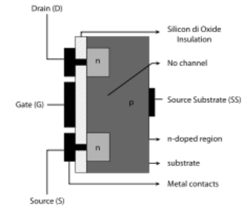
The cross section of an NMOS without channel formed: OFF state
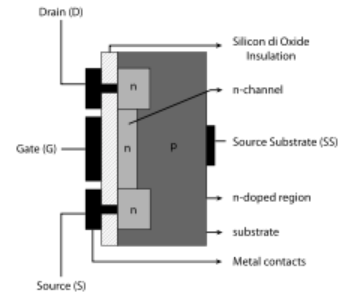
The cross section of an NMOS with channel formed: ON state
The metal-oxide-semiconductor field effect transistor (MOSFET) is based on modulation of the charge concentration by a MOS capacitance in between a body electrode and a gate electrode located above body and insulated from all the other device regions by a gate dielectric layer which in the case of a MOSFET is an oxide, like silicon dioxide. If dielectrics other than an oxide like silicon dioxide (generally referred to as oxide) are employed the device may be referred to as a metal-insulator-semiconductor FET (MISFET). Compared to MOS capacitor, the MOSFET includes 2 additional terminals (source and drain), each connected to the individual highly doped regions that are separated by the body region. These regions can be either P or N type, but they should both be of same type, and of opposite type to the body region. The source and drain are highly doped as signified by a '+' sign after the type of doping.
If MOSFET is an N channel or nMOS FET, then the source and drain are 'n+' regions and the body is a 'p' region. As described above, with sufficient gate voltage, holes from the body are driven away from gate, forming an inversion layer or N channel at the interface in between the p region and the oxide. This conducting channel extends in between the source and the drain, and current is conducted through it when a voltage is applied in between source and drain.
For the gate voltages below the threshold value, the channel is slightly populated, and only a very small subthreshold leakage current can flow in between the source and the drain.
If MOSFET is a P channel or pMOS FET, the source and drain are then 'p+' regions and the body is a 'n' region. When a negative gate-source voltage is applied, it creates a P channel at the surface of N region, analogous to N channel case, but with opposite polarities of the charges and voltages. When the voltage less negative than threshold value (a negative voltage for P channel) is applied in between gate and source, the channel disappears and a very small subthreshold current can only flow in between source and drain.
The source is so named as it is the source of the charge carriers (electrons for Nchannel, holes for N channel) which flow through the channel; likewise, the drain is where the charge carriers leave channel.
The device can comprise a Silicon On Insulator (SOI) device in which the Buried OXide (BOX) is formed below the thin semiconductor layer. If the channel region in between the gate dielectric and a Buried Oxide (BOX) region is thin, the thin channel region is referred to as an Ultra Thin Channel (UTC) region with source and drain regions formed on either side thereof in and above the thin semiconductor layer. Alternatively, the device can comprise a SEMiconductor On Insulator (SEMOI) device in which the semiconductors except silicon are employed. Many alternative semiconductor materials can be employed.
When source and drain regions are formed above channel in whole or in part, they are referred as Raised Source/Drain (RSD) regions.
Email based Electronics Devices and circuits assignment help - homework help at Expertsmind
Are you searching Electronics Engineering assignment help expert for help with MOSFET structure and channel formation questions? MOSFET structure and channel formation topic is not easier to learn without any external help? We at www.expertsmind.com offers free lecture notes for Electronics Devices and circuits assignment help and Electronics Devices and circuits homework help. Live tutors are available 24x7 hours for helping students in their MOSFET structure and channel formation related problems. We provide step by step MOSFET structure and channel formation question's answers with 100% plagiarism free content. We prepare quality content and notes for MOSFET structure and channel formation topic under Electronics Devices and circuits theory and study material. These are avail for subscribed users and they can get advantages anytime.
Why Expertsmind for assignment help
- Higher degree holder and experienced experts network
- Punctuality and responsibility of work
- Quality solution with 100% plagiarism free answers
- Time on Delivery
- Privacy of information and details
- Excellence in solving electronics engineering questions in excels and word format.
- Best tutoring assistance 24x7 hours