Full Wave Rectifier
In the earlier Power Diodes tutorial we discussed ways of reducing ripple or voltage variations on a direct DC voltage by connecting the capacitors across load resistance. While this process may be suitable for low power applications it is inappropriate to applications which require a "steady and smooth" DC supply voltage. One process to improve on this is to use every half- cycle of input voltage instead of every other half-cycle. The circuit which lets us to do this is called as Full Wave Rectifier.
Similar to the half wave circuit, a full wave rectifier circuit generates an output voltage or current which is purely DC or has some specific DC component. Full wave rectifiers have fundamental advantages over their half wave rectifier counterparts. The average (DC) output voltage is higher than for the half wave, output of the full wave rectifier has less ripple than that of half wave rectifier producing the smoother output waveform.
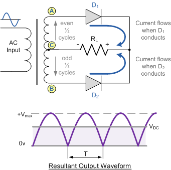
In the Full Wave Rectifier circuit 2 diodes are now used, one for each half of cycle. A transformer is used whose secondary winding is divided equally into two halves with the common centre tapped connection, (C). This configuration results in each diode conducting in turn when the anode terminal is positive with respect to transformer centre point C producing an output during both half-cycles, twice that for half wave rectifier so it is 100 per cent efficient as given below.
Full Wave Rectifier Circuit

The full wave rectifier circuit comprises of 2 power diodes connected to the single load resistance (RL) with each diode taking it in turn to supply current to load. When the point A of transformer is positive with respect to the point B, diode D1 conducts in forward direction as signified by the arrows. When point B is positive with respect to the point A, diode D2 conducts in forward direction and current flowing through resistor R is in the same direction for both the circuits. As the output voltage across the resistor R is the phase or sum of 2 waveforms combined, this kind of full wave rectifier circuit is also called as a "bi-phase" circuit.
As spaces among the each half-wave developed by each diode is now getting filled in by the other diode the average DC output voltage across load resistor is now twice that of the single half-wave rectifier circuit and is around 0.637Vmax of peak voltage, supposing no losses. However in reality, during the each half cycle current flows through two diodes instead of one so the amplitude of the output voltage is 2 voltage drops ( 2 x 0.7 = 1.4V ) less than input VMAX amplitude.

The peak voltage of output waveform is same as before for the half-wave rectifier provided each half of the transformer windings have the same rms voltage value. To obtain a different DC voltage output different transformer ratios can be used. The main disadvantage of this type of full wave rectifier circuit is that a larger transformer for a given power output is required with two separate but identical secondary windings making this type of full wave rectifying circuit costly compared to the "Full Wave Bridge Rectifier" circuit equivalent.
Email based Electronics Devices and circuits assignment help - homework help at Expertsmind
Are you searching Electronics Engineering assignment help expert for help with Full Wave Rectifier questions? Full Wave Rectifier topic is not easier to learn without any external help? We at www.expertsmind.com offers free lecture notes for Electronics Devices and circuits assignment help and Electronics Devices and circuits homework help. Live tutors are available 24x7 hours for helping students in their Full Wave Rectifier related problems. We provide step by step Full Wave Rectifier question's answers with 100% plagiarism free content. We prepare quality content and notes for Full Wave Rectifier topic under Electronics Devices and circuits theory and study material. These are avail for subscribed users and they can get advantages anytime.
Why Expertsmind for assignment help
- Higher degree holder and experienced experts network
- Punctuality and responsibility of work
- Quality solution with 100% plagiarism free answers
- Time on Delivery
- Privacy of information and details
- Excellence in solving electronics engineering questions in excels and word format.
- Best tutoring assistance 24x7 hours