FET as amplifier
Similar to the Bipolar junction transistor, JFET can also be taken in use as an amplifier. The equivalent circuit of AC of a JFET is shown in the figure 1.
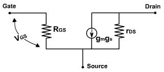
Figure 1
The resistance in between the gate and the source RGS is quite high. The drain of a JFET behaves like a current source with the value of gm Vgs. This model is applicable at the low frequencies.
From AC equivalent model
![1975_FET -amplifier2].png](https://www.expertsmind.com/../CMSImages/1975_FET -amplifier2].png)
Amplification factor µ for FET can be defined as
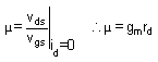
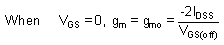
When VGS = 0, gm has its maximum value. The maximum value is designated as gmo.
Again consider the equation,
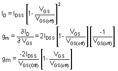
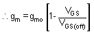
As VGS increases, gm decreases linearly.
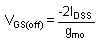
Measuring IDSS and gm, VGS(off) can be determined
Figure 2, shows the common source amplifier.
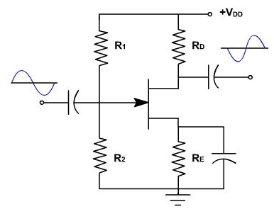
Figure 2
When a small AC signal is coupled into the gate it creates variations in gate source voltage. This generates sinusoidal drain current. As the AC current flows through the drain resistor. The amplified AC voltage is obtained at output. Increase in the gate source voltage generates more drain current, which shows that the drain voltage is decreasing. As the positive half cycle of input voltage generates the negative half cycle of output voltage, we obtain the phase inversion in a CS amplifier.
The AC equivalent circuit is shown in the figure 3.
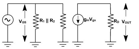
Figure 3
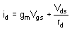
The AC output voltage can be given as vout = - gm, v gS RD
Hear the negative sign means phase inversion. Because the AC source is directly connected between the gate source terminals hence the AC input voltage equals
Vin = Vgs
The voltage gain can be given by
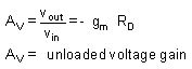
The further simplified model of the amplifiers is shown in the figure 4.
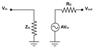
Figure 4
Hear Zin is the input impedance. At the low frequencies, this is the parallel combination of R1|| R2|| RGS. Since RGS is quite large, it is parallel combination of R1 & R2. A Vin is output voltage and RD is output impedance.
Because of the nonlinear transductance curve, the JFET distorts large signals, as shown in the figure 5.
Given a sinusoidal input voltage, we obtain a non-sinusoidal output current in which the positive half cycle is elongated and negative cycle is compressed. This kind of distortion is called as Square law distortion because transductance curve is parabolic.
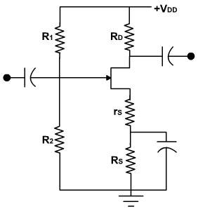
Figure 5 Fig. 6
The distortion is undesirable for an amplifier. One method to minimize this is to keep the signal small. In that case the part of curve is used and operation is nearly linear. At times swamping resistor is taken in use to minimize the distortion and gain constant. Now source is no longer AC ground as shown in the figure 6.
Drain current through rS produces an AC voltage in between the source and ground. If rS is large sufficiently the local feedback can swamp out non-linearity of the curve. Then the voltage gain reaches the ideal value of RD / rS.
Since RGS reaches infinity thus, all the drain current flows through rS producing a voltage drop of gm VgS rS. The Ac equivalent circuit is shown in the figure 7.
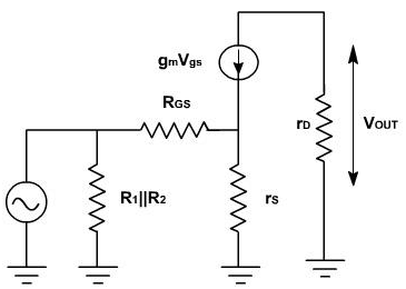
Fig. 7
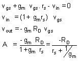
The voltage gain decreases but voltage gain is quite less effective by making change in gm. rS should be greater than 1 / gm only then

Email based Electronics Devices and circuits assignment help - homework help at Expertsmind
Are you searching Electronics Engineering assignment help expert for help with Field Effect Transistor as Amplifier questions? Field Effect Transistor as Amplifier topic is not easier to learn without any external help? We at www.expertsmind.com offers free lecture notes for Electronics Devices and circuits assignment help and Electronics Devices and circuits homework help. Live tutors are available 24x7 hours for helping students in their Field Effect Transistor as Amplifier related problems. We provide step by step Field Effect Transistor as Amplifier question's answers with 100% plagiarism free content. We prepare quality content and notes for Field Effect Transistor as Amplifier topic under Electronics Devices and circuits theory and study material. These are avail for subscribed users and they can get advantages anytime.
Why Expertsmind for assignment help
- Higher degree holder and experienced experts network
- Punctuality and responsibility of work
- Quality solution with 100% plagiarism free answers
- Time on Delivery
- Privacy of information and details
- Excellence in solving electronics engineering questions in excels and word format.
- Best tutoring assistance 24x7 hours