Emitter Follower Regulator:
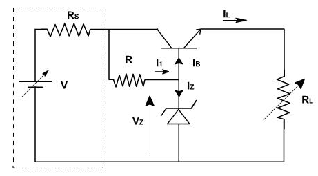
To get a better voltage regulation in shunt regulator, the zener diode can be connected to base circuit of a power transistor as shown in the figure 1. This amplifies zener current range. It is also called as emitter follower regulation.

Fig. 1
This configuration reduces current flow in the diode. The power transistor used in this configuration is called as pass transistor. The purpose of CL is to ensure that the variations in one of the regulated power supply loads will not be fed to other loads. i.e. capacitor effectively shorts out high-frequency variations.
Due to the current amplifying property of transistor, the current in zenor dioide is small. Hence there is less voltage drop across the diode resistance, and zener approximates an ideal constant voltage source.
Operation of the circuit:
The current through resistor R is sum of the zener current IZ and the transistor base current IB ( = IL / β ).
IL = IZ + IB
The output voltage across RL resistance is given by
VO = VZ - VBE
Where VBE ? 0.7 V
Therefore, VO= constant.
The emitter current and load current are same. The current IR is supposed to be constant for a given supply voltage. Thus, if IL increases, it requires more base currents, to increase base current Iz decreases. The difference in this regulator with the zener regulator is that in later case zener current decreases by same amount by which the load current increases.Thus the current range is less, while in shunt regulators, if IL increases by ΔIL then IB must increase by ΔIL / β or IZ should decrease by ΔIL / β. Thus the current range control is more for same rating zener.
The simplified circuit of shunt regulator is shown in the figure 2.

Fig.2
In the power supply power regulation is basically, because of its elevated internal impedance. In circuit discussed, the unregulated supply has resistance RS of the order of 100 ohm. The use of emitter follower is to reduce output resistance and it becomes nearly.
RO = ( Rz + hie ) / (1 + hfe)
Here RZ represents dynamic zener resistance. The voltage stabilization ratio SV is
SV = ∂ Vo / ∂ VI = Rz / (Rz + R)
The SV can be improved by increasing R. This increases VCE and power dissipated in transistor. Other disadvantages of circuit are.
1. No stipulation for varying the output voltage since it is almost equal to zener voltage.
2. Change in the VBE and Vz because of temperature variations appear at output since the transistor is connected in series with the load, it is called as series regulator and transistor is the allow series pass transistor.
Email based Electronics Devices and circuits assignment help - homework help at Expertsmind
Are you searching Electronics Engineering assignment help expert for help with Emitter Follower Regulator questions? Emitter Follower Regulator topic is not easier to learn without any external help? We at www.expertsmind.com offers free lecture notes for Electronics Devices and circuits assignment help and Electronics Devices and circuits homework help. Live tutors are available 24x7 hours for helping students in their Emitter Follower Regulator related problems. We provide step by step Emitter Follower Regulator question's answers with 100% plagiarism free content. We prepare quality content and notes for Emitter Follower Regulator topic under Electronics Devices and circuits theory and study material. These are avail for subscribed users and they can get advantages anytime.
Why Expertsmind for assignment help
- Higher degree holder and experienced experts network
- Punctuality and responsibility of work
- Quality solution with 100% plagiarism free answers
- Time on Delivery
- Privacy of information and details
- Excellence in solving electronics engineering questions in excels and word format.
- Best tutoring assistance 24x7 hours