Introduction to depletion layer pn junction:
If the one side of crystal pure semiconductor Si(silicon) or Ge(Germanium) is doped with the acceptor impurity atoms and other side is doped with donor impurity atoms , a PN junction is formed as shown in figure. P region has high concentration of holes and N region contains large the number of electrons.
What is Depletion Layer of PN Junction?
When the junction is formed, free electrons and holes cross through junction by the process of diffusion. Throughout this process, the electrons crossing junction from N- region into P-region , recombine with the holes in P-region very close to junction. Likewise holes crossing the junction from P-region into N-region, recombine with the electrons in N- region very close to junction. Thus the region is formed, which does not contain any mobile charge very close to the junction. This region is called as depletion layer of PN junction.
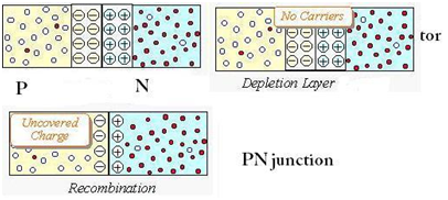
In this region, on left side of the junction, the acceptor atoms become negative ions and on the right side of the junction, the donor atoms become positive ions as shown in figure.
Email based Electronics Devices and circuits assignment help - homework help at Expertsmind
Are you searching Electronics Engineering assignment help expert for help with Depletion Layer of PN Junction questions? Depletion Layer of PN Junction topic is not easier to learn without any external help? We at www.expertsmind.com offers free lecture notes for Electronics Devices and circuits assignment help and Electronics Devices and circuits homework help. Live tutors are available 24x7 hours for helping students in their Depletion Layer of PN Junction related problems. We provide step by step Depletion Layer of PN Junction question's answers with 100% plagiarism free content. We prepare quality content and notes for Depletion Layer of PN Junction topic under Electronics Devices and circuits theory and study material. These are avail for subscribed users and they can get advantages anytime.
Why Expertsmind for assignment help
- Higher degree holder and experienced experts network
- Punctuality and responsibility of work
- Quality solution with 100% plagiarism free answers
- Time on Delivery
- Privacy of information and details
- Excellence in solving electronics engineering questions in excels and word format.
- Best tutoring assistance 24x7 hours