Current-voltage characteristic
A semiconductor diode's behavior in the circuit can be given by its current-voltage characteristic, or I- V graph (graph given below). The shape of the curve can be determined by the transport of charge carriers through the depletion layer or depletion region which exists at p-n junction between differing semiconductors. When the p-n junction is first created, conduction band (mobile) electrons from N-doped region diffuse into P-doped region where there is a large population of the holes (vacant places for electrons) with which electrons -recombine. When the mobile electron recombines with a hole, hole and electron both vanish, leaving behind the immobile positively charged donor (dopant) on N-side and negatively charged acceptor (dopant) on P-side. The region around p-n junction becomes depleted of charge carriers and therefore behaves as an insulator.
But, the width of the depletion region (called as depletion width) cannot grow without limit. For each electron-hole pair which recombines, a positively charged dopant ion is left behind in N-doped region, and a negatively charged dopant ion is left behind in P-doped region. As recombination progresses more ions are generated, an increasing electric field develops through depletion zone which acts to slow and then finally stop recombination. Now at this point, there is a built in potential across depletion zone.
If the external voltage is placed across diode with the same polarity as the built-in potential, depletion zone continues to behave as an insulator, preventing any important electric current flow (unless electron/hole pairs are actively being created in the junction by, such as light. This is the reverse bias phenomenon. However, if the polarity of the external voltage opposes the built-in potential, recombination can once again progress, resulting in substantial electric current through the p-n junction (that is substantial numbers of electrons and holes recombine at the junction). For the silicon diodes, the built-in potential is approximately 0.7 V (0.3 V for Germanium and 0.2 V for Schottky). Therefore, if an external current is passed through diode, about 0.7 V will be developed across diode so that the P-doped region is positive with respect to N-doped region and the diode is said to be -turned on as it has a forward bias.
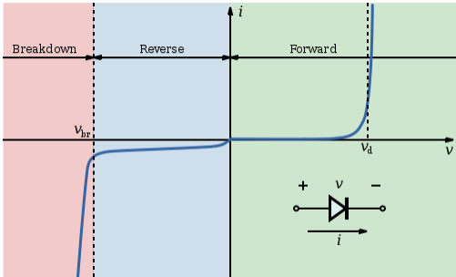
Figure- I-V characteristics of the P-N junction diode.
A diode's 'I-V characteristic' can be approximated by four regions of operation (see the figure at right).
At quite large reverse bias, beyond the peak inverse voltage or PIV, a process called as reverse breakdown occurs which creats a large increase in current (that is a large number of electrons and holes are created at, and move away from PN junction) which usually damages the device permanently. The avalanche diode is deliberately designed for the use in avalanche region. In the zener diode, the concept of PIV is not applicable. A zener diode comprises a heavily doped p-n junction allowing the electrons to tunnel from valence band of the p-type material to the conduction band of n-type material, so that the reverse voltage is -clamped to a known value (called as zener voltage), and avalanche does not take place. Both devices, do have a limit to the maximum current and power in clamped reverse voltage region. Also, following end of forward conduction in any diode, there is reverse current for the short time. The device does not achive its full blocking capability until reverse current ceases.
The second region, at the reverse biases more positive than PIV, has only a small reverse saturation current. In reverse bias region for a normal P-N rectifier diode, the current through the device is quite low (in µA range). However, this is temperature dependent, and at sufficiently high temperatures, a substantial amount of the reverse current can be observed (mA or more).
The third region is forward but small bias, where only the small forward current is conducted.
As potential difference is increased above the arbitrarily defined cut in voltage or on voltage or diode forward voltage drop (denoted by Vd), the diode current becomes appreciable (the level of current considered appreciable and the value of cut-in voltage depends on the application), and diode presents a very low resistance. The current-voltage curve is exponential in nature. In the normal silicon diode at rated currents, the arbitrary cut in voltage can be defined as 0.6 to 0.7 volts. The value is different for the other diode types - Schottky diodes can be rated as low as 0.2 V, Germanium diodes 0.25-0.3 V, and the red or blue light emitting diodes (LEDs) can have values of 1.4 V and 4.0 V respectively.
At the higher currents forward voltage drop of the diode increases. A drop of 1 V to 1.5 V is distinctive at the full rated current for power diodes.
Email based Electronics Devices and circuits assignment help - homework help at Expertsmind
Are you searching Electronics Engineering assignment help expert for help with Current–voltage characteristic questions? Current–voltage characteristic topic is not easier to learn without any external help? We at www.expertsmind.com offers free lecture notes for Electronics Devices and circuits assignment help and Electronics Devices and circuits homework help. Live tutors are available 24x7 hours for helping students in their Current–voltage characteristic related problems. We provide step by step Current–voltage characteristic question's answers with 100% plagiarism free content. We prepare quality content and notes for Current–voltage characteristic topic under Electronics Devices and circuits theory and study material. These are avail for subscribed users and they can get advantages anytime.
Why Expertsmind for assignment help
- Higher degree holder and experienced experts network
- Punctuality and responsibility of work
- Quality solution with 100% plagiarism free answers
- Time on Delivery
- Privacy of information and details
- Excellence in solving electronics engineering questions in excels and word format.
- Best tutoring assistance 24x7 hours