Common Emitter Configuration
Output Characteristic:
The output characteristic is curve between VCE and IC for the various values of IB. For the constant value of IB and is shown in the figure 3. For the fixed value of IB, IC is not varying much dependent on VCE but slopes are greater than characteristic of CE. The output characteristics can be divided into 3 parts.
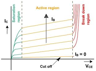
Fig.
(1) Active Region:
In this region the collector junction is reverse biased and the emitter junction is forward biased. It is the area to right of VCE = 0.5 V and above IB= 0. In this area the transistor current responds very sensitively to IB. If the transistor is to be used as an amplifier, it should operate in this region.
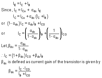
If αdc is truly constant then IC would be independent of VCE. But due to early effect, αdc increases by 0.1% (0.001) for example from 0.995 to 0.996 as VCE increases from a few volts to 10V. Then bdc increases from 0.995 / (1-0.995) = 200 to 0.996 / (1-0.996) = 250 or about 25 per cent. This shows that small change in the a reflects large change in b. Thus the curves are subjected to large variations for same type of the transistors.
(2) Cut Off:
Cut off in a transistor can be given by IB = 0, IC= ICO. A transistor is not at cut off if base current is simply reduced to zero under this condition,
IC = IE= ICO / ( 1-αdc) = ICEO
The actual collector current with the base open is designated as ICEO. As even in neighborhood of cut off, a dc can be as large as 0.9 for Ge, then IC=10 ICO, at zero base current. Accordingly in order to cut off transistor it is not sufficient to reduce IB to zero, but it is also necessary to reverse bias the emitter junction a little. It is found that the reverse voltage of 0.1 V is sufficient for the cut off a transistor. In Si, the a dc is nearly equal to zero, hence, IC = ICO. Hence even with IB= 0, IC= IE= ICO so that transistor is quite close to cut off. The cut off means IE = 0, IC = ICO, IB = -IC = -ICO, and VBE is a reverse voltage whose magnitude is of order of 0.1 V for Ge and 0 V for Si.
Reverse Collector Saturation Current ICBO:
In the physical transistor when the emitter current is reduced to zero, then collector current is called as ICBO (nearly equal to ICO). Reverse collector saturation current ICBO also varies with avalanche multiplication, temperature, and variability of each sample. Consider the circuit shown in the fifure 4. VBB is reverse voltage applied to reduce emitter current to zero. IE = 0, IB = -ICBO
If we need, VBE = - 0.1 V Then - VBB + ICBO RB < - 0.1 V
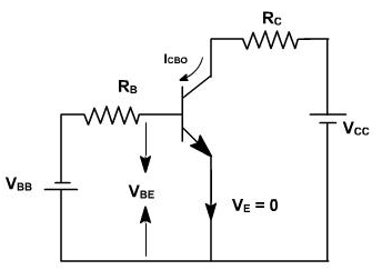
Figure 4
If RB = 100 K, ICBO = 100 m A, then VBB should be 10.1 Volts. Hence transistor should be capable to withstand this reverse voltage before the breakdown voltage exceeds.
(3).Saturation Region:
In this region both diodes are forward biased by at least cut in voltage. As the voltage VBE and VBC across a forward is approximately 0.7 V therefore, VCE = VCB + VBE = - VBC + VBE is few tenths of volts. Hence the saturation region is quite close to zero voltage axis, here all the current quickly reduces to zero. In this region transistor collector current is approximately can be given by VCC / R C and independent of base current. The normal transistor action is last and it behaves like a small ohmic resistance.
Email based Electronics Devices and circuits assignment help - homework help at Expertsmind
Are you searching Electronics Engineering assignment help expert for help with Common Emitter Configuration - Output Characteristic questions? Common Emitter Configuration - Output Characteristic topic is not easier to learn without any external help? We at www.expertsmind.com offers free lecture notes for Electronics Devices and circuits assignment help and Electronics Devices and circuits homework help. Live tutors are available 24x7 hours for helping students in their Common Emitter Configuration - Output Characteristic related problems. We provide step by step Common Emitter Configuration - Output Characteristic question's answers with 100% plagiarism free content. We prepare quality content and notes for Common Emitter Configuration - Output Characteristic topic under Electronics Devices and circuits theory and study material. These are avail for subscribed users and they can get advantages anytime.
Why Expertsmind for assignment help
- Higher degree holder and experienced experts network
- Punctuality and responsibility of work
- Quality solution with 100% plagiarism free answers
- Time on Delivery
- Privacy of information and details
- Excellence in solving electronics engineering questions in excels and word format.
- Best tutoring assistance 24x7 hours