Bipolar transistor:
A transistor is generally a Si on Ge crystal having three separate regions. It can either be NPN or PNP type figure1. The middle region is called as base and the outer two regions are called as emitter and the collector. The outer layers although they are of the same type but their functions can't be changed. They have different physical and electrical properties both.
In most of the transistors, emitter is very heavily doped. Its job is to emit or inject electrons into base. These bases are slightly doped and very thin, it passes most of the emitter injected electrons on to the collector. The doping level of collector is intermediate between the heavy doping of emitter and the light doping of base.
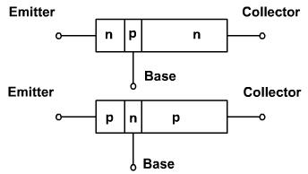
Fig. 1
The collector is named so because it collects electrons from the base. The collector is largest of the three regions; it must dissipate more heat than emitter or base. The transistor has 2 junctions. One between emitter and base and other between base and collector. Because of this the transistor is similar to two diodes, one emitter diode and the other collector base diode.
The depletion layers don't have the same width, because different regions have different doping levels. The more heavily doped a region is, greater the concentration of ions near the junction. This means that the depletion layer penetrates more deeply into the base and slightly into the emitter. Likewise, it penetration more into collector. The thickness of the collector depletion layer is large while the base depletion layer is small as shown in the figure 2.
When a transistor is made, diffusion of the free electrons across junction produces two depletion layers. For each of the depletion layers, the barrier potential is 0.7 V for Si transistor and 0.3 V for the Ge transistor.
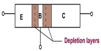
Figure 2
If both the junctions are forward biased using 2 DC sources, as shown in the figure 3a. free electrons enter emitter and collector of transistor, joins at base and come out of base. Because both the diodes are forward biased, emitter and collector currents are large.
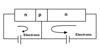
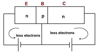
Fig. 3a Fig. 3b
If both the junction are reverse biased as shown in the figure 3b, then small currents flows through both junctions only because of thermally produced minority carriers and surface leakage. Thermally produced carriers are temperature dependent it nearly doubles for every 10 degree Celsius rise in the ambient temperature. The surface leakage current increases with voltage.
When emitter diode is forward biased and collector diode is reverse biased as shown in the figure 4 then one expect the large emitter current and small collector current but collector current is almost as large as the emitter current.
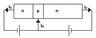
Figure 4
When the emitter diodes are forward biased and the applied voltage is over 0.7 V (barrier potential) then the larger number of majority carriers (electrons in N type) diffuse across the junction.
Once the electrons are injected by emitter enter into base, they become minority carriers. These electrons don't have separate identities from those, which are generated thermally, in the base region itself. The base is made quite thin and is very lightly doped. Because of this only few electrons traveling from emitter to base region recombine with the holes. This gives rise to the recombination current. The rest of the electrons exist for more time. Since the collector diode is reverse biased, (n is connected to the positive supply) thus most of the electrons are pushed into collector layer. These collector elections can then flow into external collector lead.
Therefore, there is a steady stream of the electrons leaving negative source terminal and entering emitter region. The VEB forward bias forces these emitter electrons to enter the base region. The thin and lightly doped base gives almost all those electrons enough lifetime to diffuse into depletion layer. The depletion layer field pushes a steady stream of electron into the collector region. These electrons leave the collector and flow into the positive terminal of the voltage source. In most of the transistors, over 95% of the emitter injected electrons flow to collector, below 5% fall into base holes and flow out the external base lead. But the collector current is below emitter current.
Email based Electronics Devices and circuits assignment help - homework help at Expertsmind
Are you searching Electronics Engineering assignment help expert for help with Bipolar Transistor questions? Bipolar Transistor topic is not easier to learn without any external help? We at www.expertsmind.com offers free lecture notes for Electronics Devices and circuits assignment help and Electronics Devices and circuits homework help. Live tutors are available 24x7 hours for helping students in their Bipolar Transistor related problems. We provide step by step Bipolar Transistor question's answers with 100% plagiarism free content. We prepare quality content and notes for Bipolar Transistor topic under Electronics Devices and circuits theory and study material. These are avail for subscribed users and they can get advantages anytime.
Why Expertsmind for assignment help
- Higher degree holder and experienced experts network
- Punctuality and responsibility of work
- Quality solution with 100% plagiarism free answers
- Time on Delivery
- Privacy of information and details
- Excellence in solving electronics engineering questions in excels and word format.
- Best tutoring assistance 24x7 hours