Active-mode NPN transistors in circuits
The structure and use of NPN transistor. Arrow according to representation.
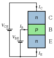
The diagram opposite is the representation of the NPN transistor connected to two voltage sources. To make transistor conduct appreciable current (on order of 1 mA) from C to E, VBE should be above a minimum value at times referred to as cut-in voltage. The cut-in voltage is usually around 600 mV for silicon BJTs at the room temperature but can be different depending on type of transistor and its biasing. This applied voltage causes lower P-N junction to 'turn-on' allowing the flow of electrons from emitter into the base. In active mode, the electric field prevailing between base and collector (cerated by VCE) will cause the majority of these electrons to cross upper P-N junction into the collector to form the collector current IC. The remainder of electrons recombines with the holes, the majority carriers in base, making a current through the base connection to form base current, IB. As shown in diagram, emitter current, IE, is total transistor current, which is sum of the other terminal currents (i.e., IE = IB + IC ).
In diagram, the arrows representing current point in the direction of conventional current -flow of the electrons is in opposite direction of the arrows cause the electrons have negative electric charge. In the active mode, ratio of collector current to base current is called as DC current gain. This gain is nearly 100 or more, but robust circuit designs do not depend on the exact value (for instance see op-amp). The value of this gain for DC signals is referred as hFE, and the value of this gain for AC signals is referred to as hfe. But, when there is no particular frequency range of interest, the symbol β is used.
It should be noted that the emitter current is related to VBE exponentially. At the room temperature, an increase in VBE by about 60 mV increases the emitter current by the factor of 10. Because the base current is roughly proportional to collector and emitter currents, they vary in the same manner.
Email based Electronics Devices and circuits assignment help - homework help at Expertsmind
Are you searching Electronics Engineering assignment help expert for help with Active-mode NPN transistors in circuits questions? Active-mode NPN transistors in circuits topic is not easier to learn without any external help? We at www.expertsmind.com offers free lecture notes for Electronics Devices and circuits assignment help and Electronics Devices and circuits homework help. Live tutors are available 24x7 hours for helping students in their Active-mode NPN transistors in circuits related problems. We provide step by step Active-mode NPN transistors in circuits question's answers with 100% plagiarism free content. We prepare quality content and notes for Active-mode NPN transistors in circuits topic under Electronics Devices and circuits theory and study material. These are avail for subscribed users and they can get advantages anytime.
Why Expertsmind for assignment help
- Higher degree holder and experienced experts network
- Punctuality and responsibility of work
- Quality solution with 100% plagiarism free answers
- Time on Delivery
- Privacy of information and details
- Excellence in solving electronics engineering questions in excels and word format.
- Best tutoring assistance 24x7 hours