Common-drain circuit
A common-drain circuit is shown in the figure given below. This circuit has the collector at the signal ground. It is called a source follower.The FET is biased in the same way as for the common source and common gate circuits. In illustration, an N-channel JFET is shown, but other kind of FET could be used, reversing polarity for P-channel devices. Enhancement mode MOSFETs would require a resistor between gate and positive supply terminal (or negative terminal if MOSFET is P-channel).
The input signal passes through C2 to gate. Resistors R1 and R2 gives gate bias. Resistor R3 restricts the current. Capacitor C3 keeps drain at signal ground. Fluctuating direct current (channel current) flows through R1 as a result of input signal; this
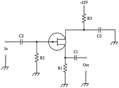
Figure-- Common-drain circuit configuration.
causes a fluctuating direct current voltage to appear across resistor. The output is taken from source, and its alternating current component passes through C1.The output of common-drain circuit is in phase with input. This scheme is FET analog of the bipolar common-collector arrangement. The output impedance is low, making this circuit a good choice for the broadband impedance matching.